0. Electronics Design & My Practice
Electronics design connects directly to what I want to build as a musician and new-media practitioner. My long-term interest is in designing custom circuit boards for instruments I'd like to create — In this first chapter of the second part of the course, we started learning how to use KiCad to design a simple PCB around the Seeed XIAO RP2040 module, which is a tiny but powerful microcontroller board with built-in USB-C and a rich set of GPIOs. It took me a day or two to get the hang of KiCad's workflow, but once I got the basics it made a lot of sense. I was thinking of 2 possibilities to design around the XIAO:
- A MIDI Bridge between two MIDI hosts (e.g. a computer running Max and a Norns sound computer).
- A custom MIDI controller with a few buttons, knobs, and an OLED display, all driven by the XIAO's GPIOs and I2C interface.
1. Schematic Design in KiCad
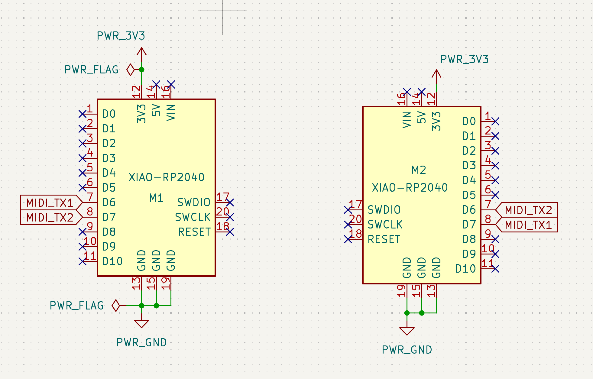
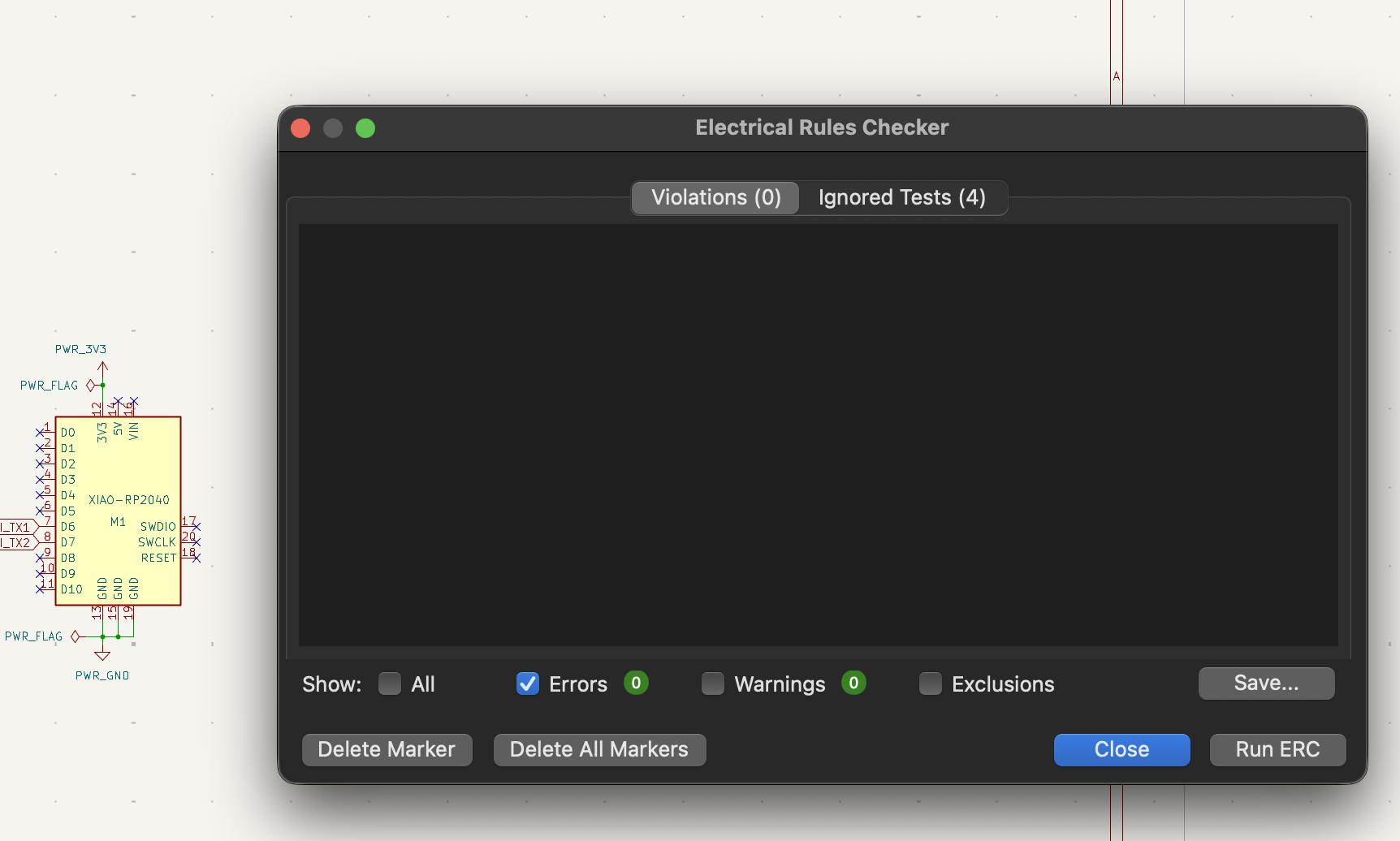
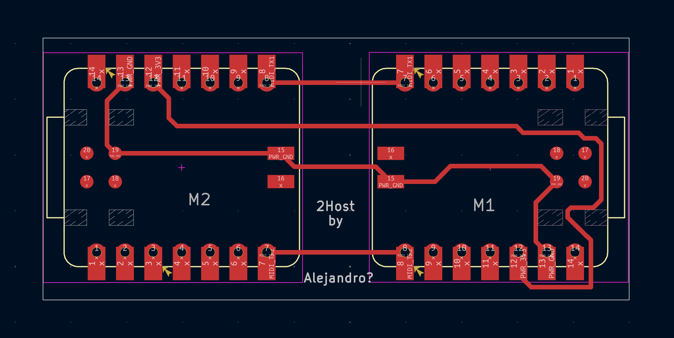
I started the schematic design, It honestly felt a bit intimidating at first, since I had never used any EDA software before, but the step-by-step tutorials provided a clear roadmap to follow. I decided to start with the MIDI Bridge concept, which is simpler and more focused on the core idea I had. So, first I layed both MCUs side by side, and did the bridge connections by connecting the ports 7 (TX) and 8 (RX) to the corresponding pins on the other MCU, this to be able to send MIDI messages between them. then I added the power supply connections (VCC and GND) to both MCUs, and a few decoupling capacitors close to their power pins for stability. In the end, I crossed all the unused connections. and ran the ERC test.
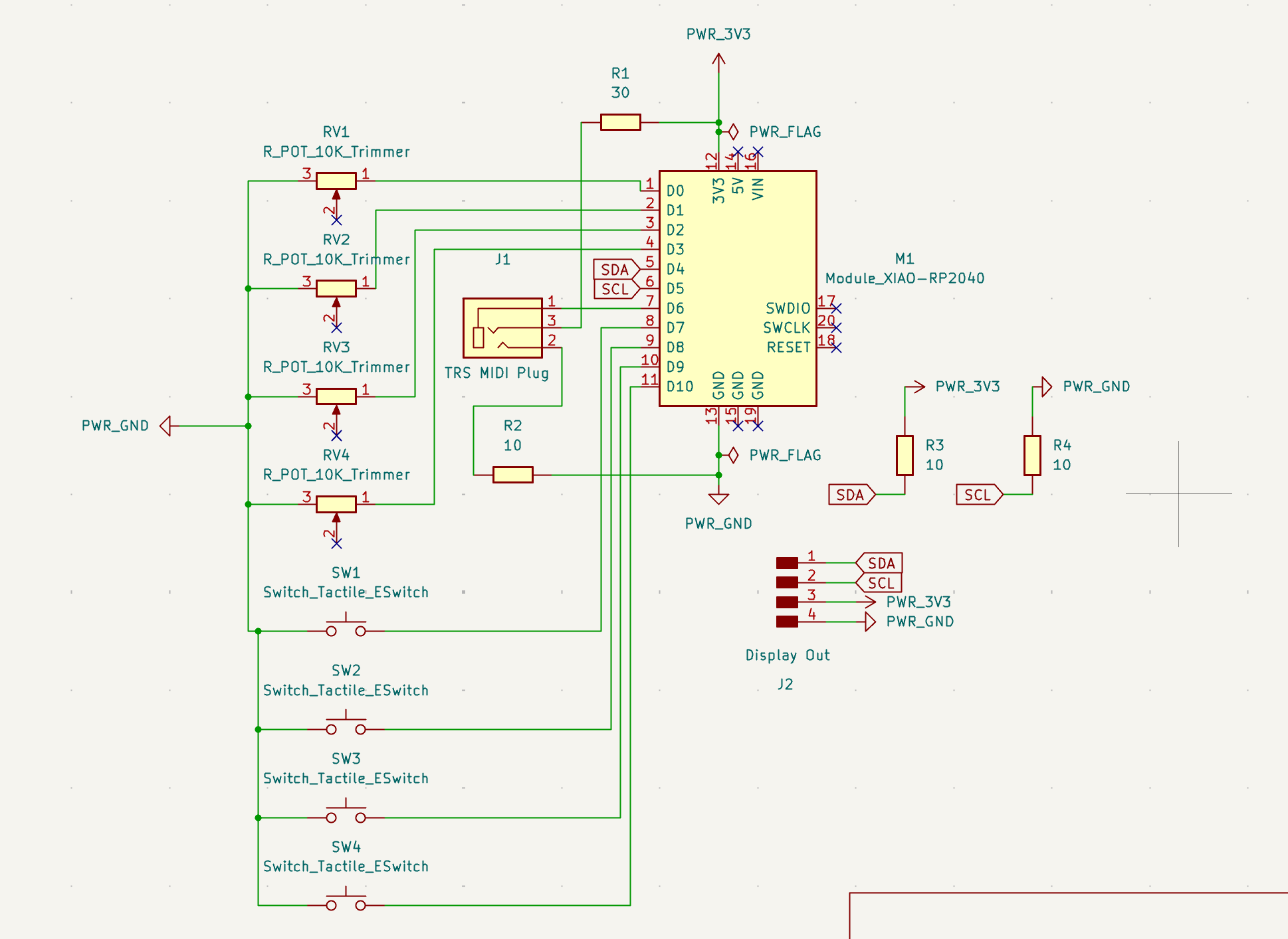
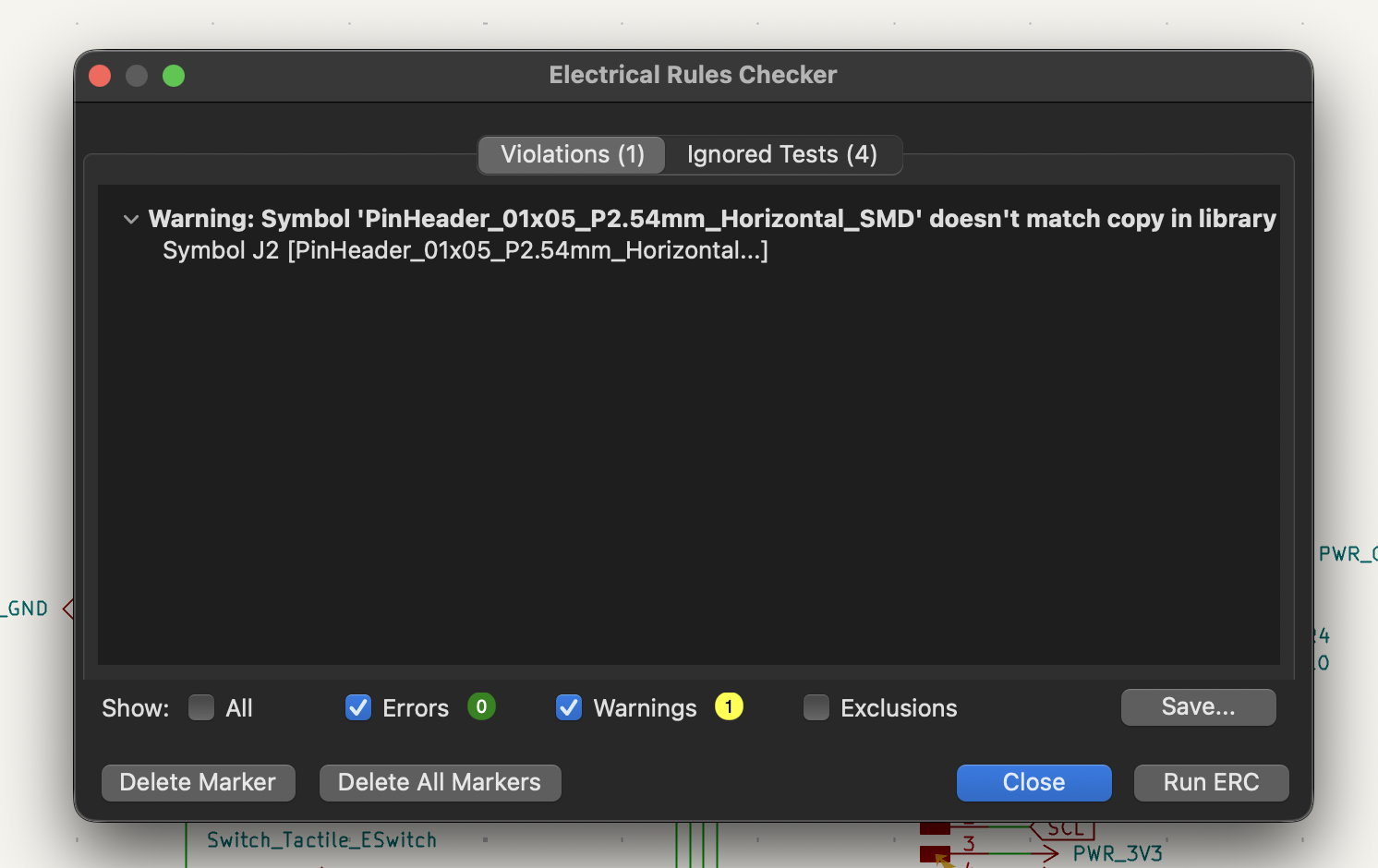
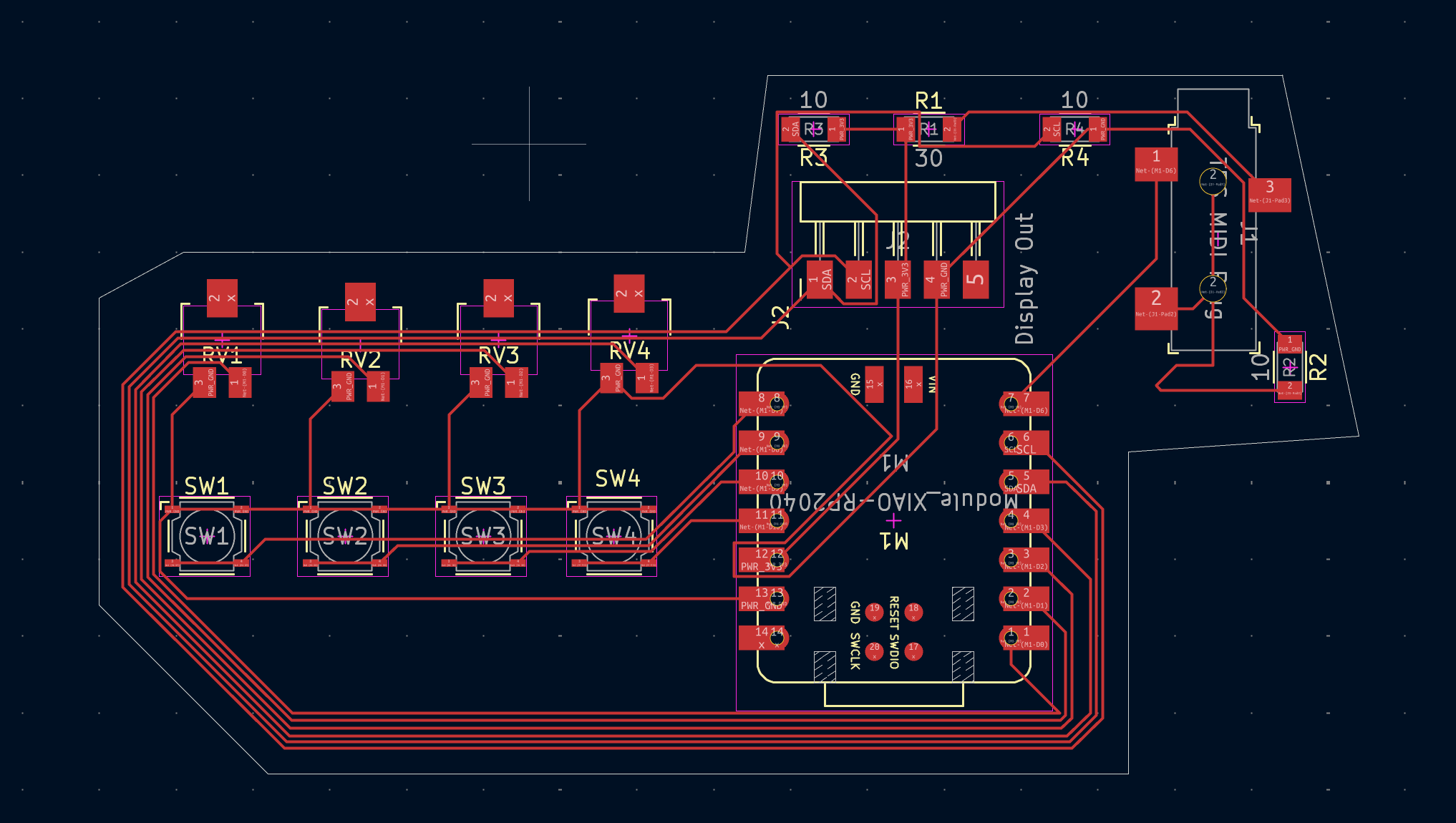
For the second design, I only needed one MCU, but I needed more components like buttons and knobs. I connected them to GPIO pins on the board and added a couple of potentiometers for analog input, and used the SCL and SDA pins for the OLED display. I also added a power switch and an LED for status indication. Again, I made sure to cross all unused connections and ran the ERC to check for errors. I wasn't sure about this design, but I did it for the assignment, and I think it could be a good starting point for a future project. Yet I believe the design is not 100% correct or usable yet.
2. PCB Layout
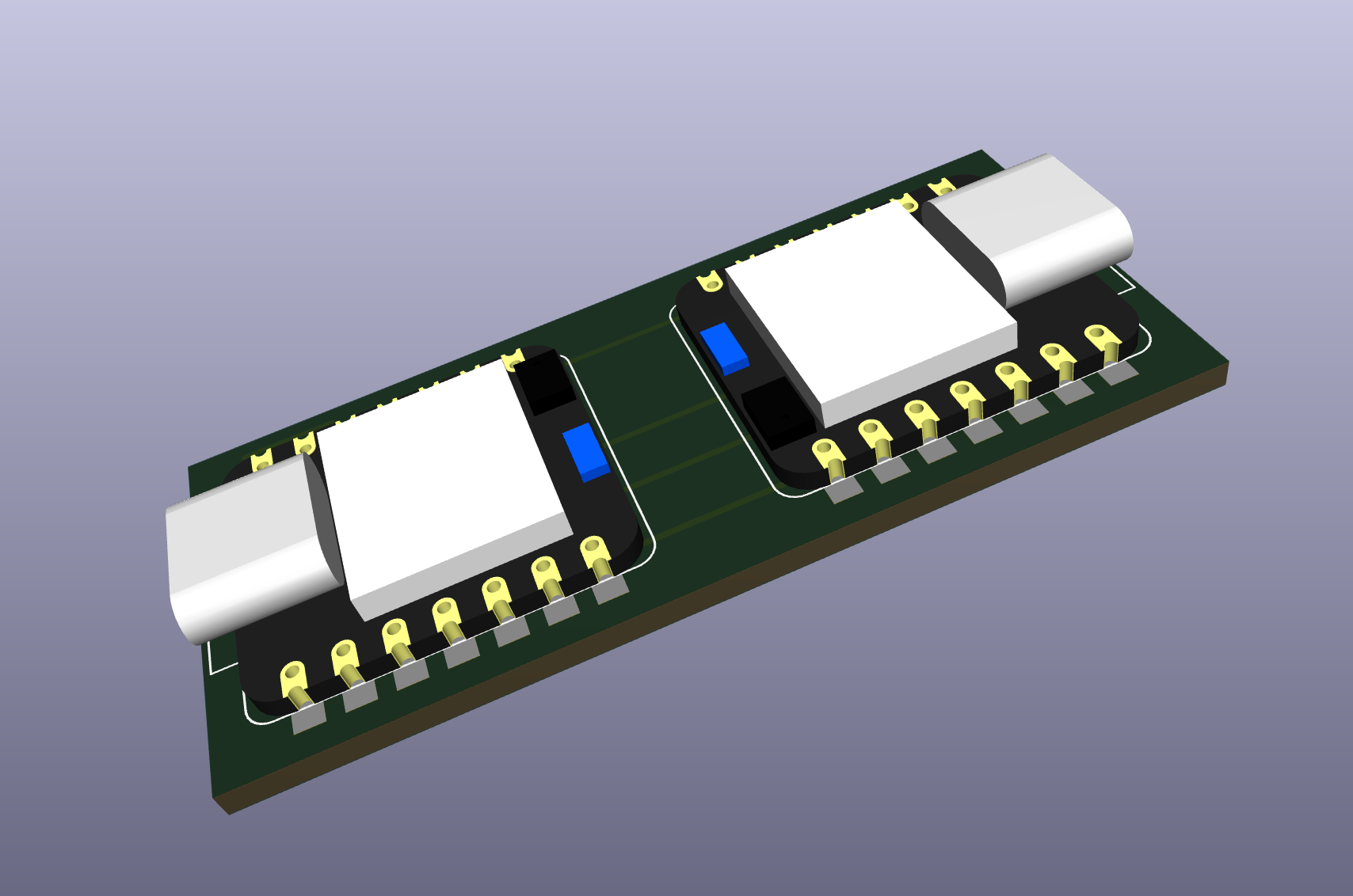
After finalizing the schematic, I moved on to the PCB layout. I imported the netlist from the schematic and started placing the components on the board. For the MIDI Bridge design, I placed the two XIAO modules on opposite sides of the board to allow for easy access to the USB ports and also ease the bridge connections. I made sure to keep the power and ground traces as short and wide as possible for better current handling.
For the MIDI controller design, I placed the XIAO and the screen in the right side of the board, with the buttons and potentiometers arranged of the left, for the fun of it. This was really just a quick layout to get a sense of how the components would fit together, and I didn't spend too much time optimizing the placement or routing. Also it became a bit of a mess, was puzzling to route the connections between the components, and I ran the DRC and tried to fix as many issues as I could, but I know there are still some problems with the layout that would need to be addressed before manufacturing. I believe also the arrange of GPIO pins I used for this was not 100% correct, but I just wanted to get a sense of how the layout process works, and I think I achieved that.
3. Exporting for Manufacturing
I exported the board as a full Gerber package suitable for JLCPCB. I made sure to include all the necessary layers, such as the copper layers, silkscreen, solder mask, and drill files. I also double-checked the design rules and ensured that all the components were properly labeled and oriented. I then uploaded the Gerber files to JLCPCB's online platform to get a quote and check for any potential issues before placing the "order" haha.
4. Project Files
Download the KiCad project files: Midi2host.zip MIDIManipulator.zip